The birth of high-brightness LED wafers, a breakthrough in new technology
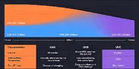
Different from the current ceramic substrate technology, the silicon substrate using the LED wafer packaging process will strongly challenge the traditional packaging process. At present, the industry is represented by TSMC's packaging plant with a semiconductor background, which specializes in wafer-level high-power LED silicon-based Packaging technology, and locked in the LED lighting market, due to the good thermal conductivity of silicon substrates, wafer-level packaging can shorten the original process, and mass production has the advantage of reducing costs, making wafer-level packaging technology aggressive and regarded as extremely Competitive technical opponents.
Xu Juemin, Dean of the Industrial Technology Research Institute, said that micro-electro-mechanical technology is the key technology in the wafer-level packaging process of today’s LED. The R&D laboratory for 8-inch MEMS wafer process technology can assist the industry in component design, manufacturing, packaging, testing, and trial mass production services.
Optimistic about the take-off of the LED lighting market in the Asia-Pacific region, Oxford Instruments officially entered the MEMS Open Laboratory of the Industrial Technology Research Institute on the 23rd to establish a R&D center, which will focus on the HB-LED (high-brightness LED) back-end wafer-level packaging process and integrate microstructure technology , Joint research and development of new and improved technologies, the technology is expected to be transferred to Taiwanese manufacturers in the future, to accelerate the improvement of the competitiveness of the LED industry,
It is reported that there are already many LED packaging related manufacturers interested in it, and it is expected that there will be major breakthroughs in silicon substrate packaging technology in the near future.
The cooperation between the Industrial Technology Research Institute and Oxford Instruments will accelerate the technology of Taiwanese manufacturers in LED wafer packaging and enhance the product competitiveness of the high-brightness LED industry in the future. The Industrial Technology Research Institute will also gradually plan for the key to micro-nano electromechanical The development of process technology has further completed Taiwan's LED and micro-nano electromechanical industry chain.
Oxford Instruments stated that it will seek suitable Taiwanese manufacturers to become its machine parts suppliers, so that the equipment can be located in Asia, and the timeliness of reducing equipment costs and speeding up production will be exerted. It is hoped that Taiwan will develop into a machine assembly center in the Asia-Pacific region in the future.
According to the Industrial Research Institute, the added value of the wafer-level packaging process is high, and each company has different designs and application technologies. At present, it has been in contact with many LED packaging factories or related industries, and it is expected that the latest technological breakthroughs will be released in the short term. , And conduct technology transfer authorization with the industry.
Since the Asia-Pacific region is the artery of the world economy, talents, and markets, and the ITRI has abundant LED R&D energy and talents, the overseas R&D center is set up in the ITRI to serve the needs of LED manufacturers in the Asia-Pacific region nearby.
Taiwan’s Ministry of Economic Affairs Technology Office stated that since the opening of direct flights between Taiwan and the United Kingdom in March 2010, they have accelerated the entry and exit of goods between the two sides and promoted business exchanges, making Taiwan a trade transshipment point for the United Kingdom to the Asia-Pacific region. With the added value of ECFA, Foreign businessmen will be able to use Taiwan as the R&D base, assembly center, and transshipment center in the Asia-Pacific region, combined with the supply chain of Taiwanese businessmen, to join hands in entering the Chinese mainland market.
The president of Oxford Instruments Group stated that Oxford Instruments has been focusing on plasma etching and chemical vapor deposition technology for more than 25 years, providing LED upstream patterned epitaxial substrates and key leading equipment for midstream die manufacturing, and cooperating with global LED manufacturers Cooperate in advanced process development to solve the problem of LED downstream packaging heat dissipation technology.